
Semiconductor Heterogeneous Integration Needs a New Kind of Wafer
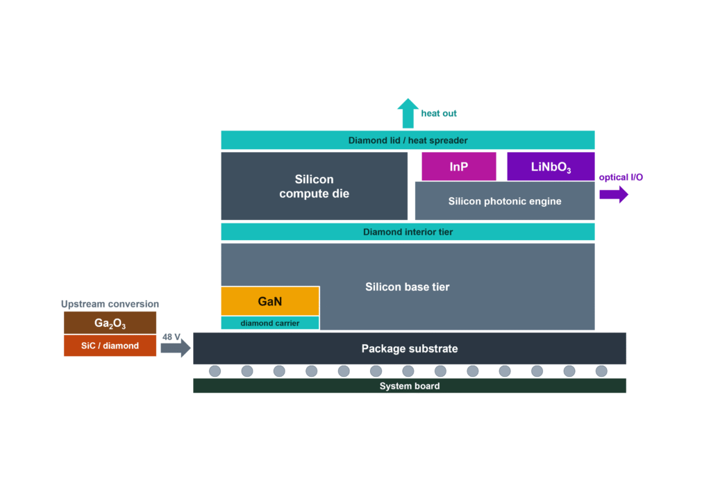
A semiconductor computing system is like a microscopic workplace. A workplace where countless employees are doing domain-specific jobs, but all deeply interconnected to create some valuable output. The workplace might be spread out in different buildings across a wide campus, or perhaps it might be occupying many consecutive floors of a skyscraper. Often it is a combination of both, depending on the cost of real estate and how particular the workspace needs to be (a specific factory layout for manufacturing versus generic offices for the sales team). For the layout of semiconductor computing chips, the ultra-dense skyscraper has become highly preferable to the sprawling campus because (1) silicon real estate is getting scarce and (2) the time information takes to travel across separate chips is becoming a massive hindrance.