November 20, 2025
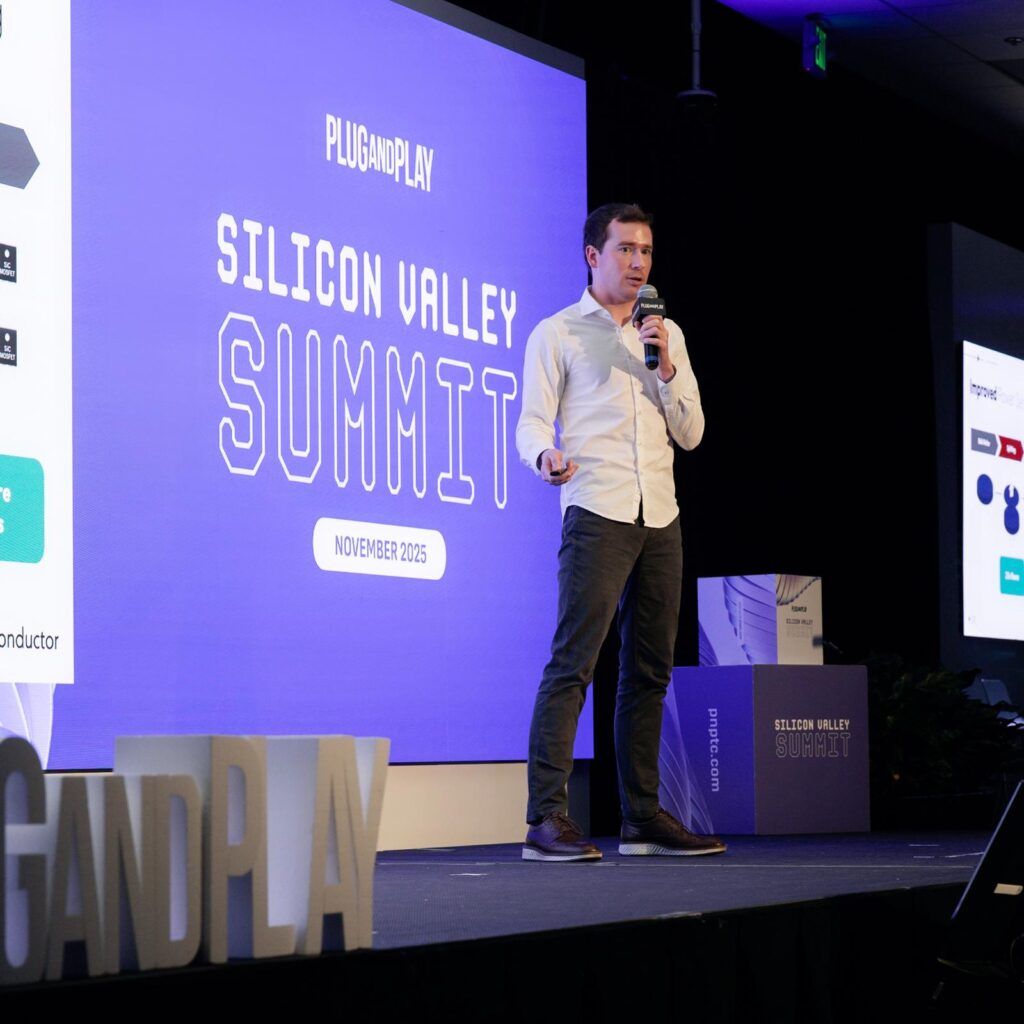
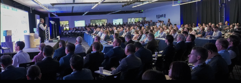
K1 Semiconductor attended the Plug and Play Tech Center’s Silicon Valley November Summit, a three-day innovation gathering featuring 300+ startups across more than 20 verticals at Plug and Play’s global headquarters in Sunnyvale, California.

The summit served as a high-energy culmination of our participation in Plug and Play’s Deep Tech Accelerator, bringing months of technical development and market validation into direct engagement with strategic partners, industry leaders, and deeptech investors.

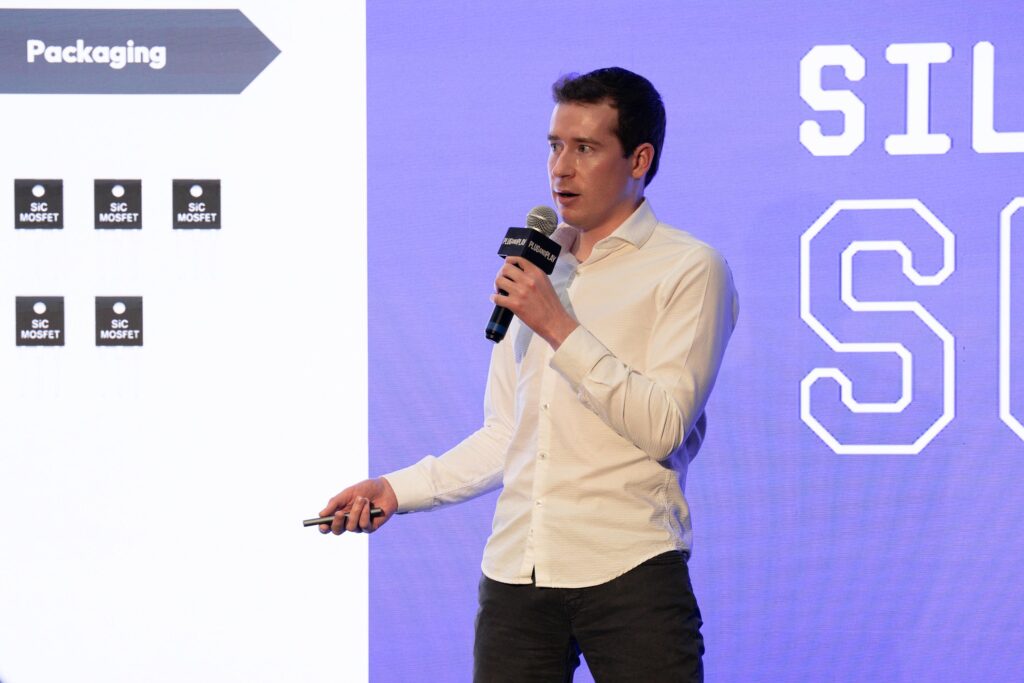
Presenting K1 Semiconductor’s Breakthrough Technology & Traction
As part of the Deeptech and Semiconductor verticals, we presented K1’s breakthrough wafer-splitting platform for advanced semiconductor materials such as SiC, GaN, and diamond. Our technology enables the reuse of high-cost substrates dramatically reducing material cost and improving manufacturing efficiency for wide-bandgap power devices.
Across conversations with engineers, corporate innovation leads, and semiconductor strategists, the same challenge surfaced: the performance benefits of wide-bandgap materials are clear but the economics and integrating them into manufacturing lines remain question marks.
Our platform technology addresses this head-on by enabling multiple device wafers to be produced from a single substrate, reshaping cost models for applications such as EV powertrains, high-efficiency converters, industrial drives, and AI data centers.

Strategic Corporate Engagement
One of the most valuable aspects of the summit was the direct interaction with key global corporate partners across the semiconductor value chain. These discussions were technical, specific, and forward-looking. Common themes emerged around:
- scaling wide-bandgap semiconductor production
- improving thermal and switching performance
- lowering cost per device through substrate efficiency
- building resilient, domestic-friendly supply chains
Several partners requested follow-up discussions, technical evaluations, and deeper collaborative exploration, including potential pilot paths, NDAs, and roadmap alignment.
High Interest From Investors
We also engaged with investors focused on semiconductor technology, advanced manufacturing, and industrial transformation. These groups increasingly recognize that major breakthroughs in the coming decade will be powered not only by software and AI but by real-world advances in materials, processes, and substrate engineering.
Many investors expressed a resonant view: the semiconductor industry is entering a new era, where value will shift from silicon saturation to wide-bandgap adoption, and the winners will be those who enable cost-effective manufacturing of high-performance semiconductors at scale.

Looking Forward
We return from Sunnyvale energized by the response to our technology and encouraged by the clear alignment between our platform and the needs of the market.
The connections made and conversations initiated at the summit will continue into the coming weeks as we deepen technical discussions, pursue strategic partnerships, and advance towards pilot deployment opportunities.
We are grateful to Plug and Play Tech Center and Aved Sodah, the program manager, for creating such a powerful platform for deeptech engagement, and we look forward to building a future where advanced semiconductors unlock innovation across industries and drive human progress.